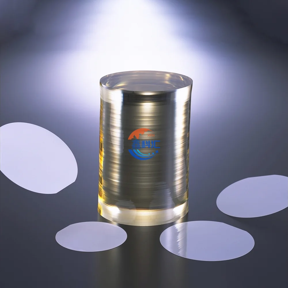
Lithium niobate crystal and wafers for optical and acoustic devices

01 / CRYSTAL WAFER PLATFORM

Lithium niobate
& lithium tantalate

Precision crystal wafers for the next generation of acoustic, optical and RF devices.

3–8 inch LiNbO33–6 inch LiTaO3Custom orientations

Made for process clarity.
One technical conversation from crystal to delivery.

01Application-led review
02Custom wafer processing
03Stable delivery planning
04Lot-level communication

02 / PRODUCT RANGE

Two crystal families.
Many device paths.

Shanghai Xinkehui New Materials Co., Ltd. supplies lithium niobate and lithium tantalate wafers for research, pilot lines and production-oriented programs. Material, cut, finish and inspection criteria are reviewed before quotation.

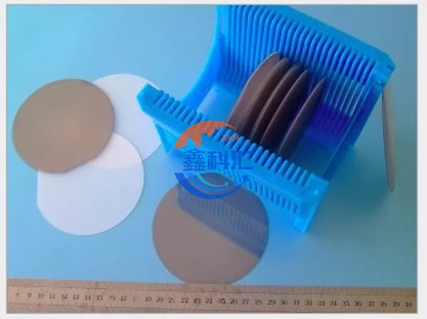
Lithium niobate wafers in a protective carrierLiNbO3 / LN

OPTICAL + PIEZOELECTRIC

Lithium niobate wafers

Nonlinear optical and electro-optic crystal wafers for waveguides, modulators, frequency conversion and SAW platforms.

  • 3, 4, 6 and 8 inch listed
  • X, Z, Y, 41°, 64°, 128° Y-cut
  • MgO / Zn doping review
See LiNbO3 parameters ↗
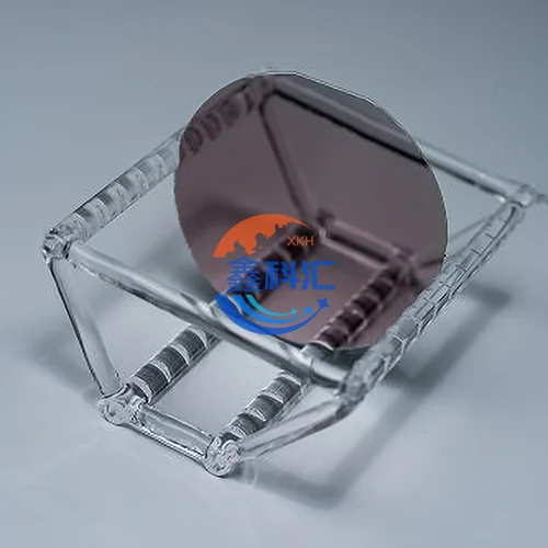
Lithium tantalate wafers for high-frequency acoustic devicesLiTaO3 / LT

STABLE ACOUSTIC PLATFORM

Lithium tantalate wafers

Piezoelectric, pyroelectric and acousto-optic material for resonators, filters, transducers and high-frequency SAW devices.

  • 3, 4 and 6 inch listed
  • X112°, Y28°, Y36°, Y42°
  • Curie temperature 605°C ± 3°C
See LiTaO3 parameters ↗

YOUR DRAWING, OUR REVIEW

Custom crystal wafers

Need a non-standard cut, thickness, edge or polish? Send a drawing, device stack or acceptance table and our team will map the practical route.

OrientationThicknessSurfaceEdge profile
Start an RFQ ↗

03 / APPLICATIONS

Materials that turn
signals into function.

The right cut and finish can influence acoustic coupling, optical interaction and process yield. Choose the application first, then specify the wafer.

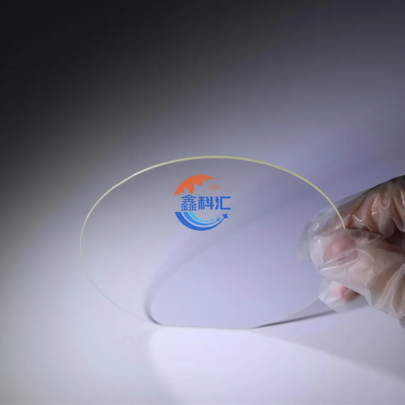
Thin lithium niobate wafer for photonic devices
01

Photonics & electro-optics

Bulk or thin-wafer routes for optical waveguides, modulators, frequency conversion and nonlinear optics.

Discuss wavelength & cut ↗
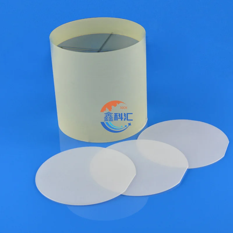
MgO doped lithium niobate crystal wafer
02

SAW filters & RF

Piezoelectric substrates for filters, resonators and front-end acoustic components in communication devices.

Discuss acoustic design ↗
Polished lithium crystal wafers for transducer research
03

Ultrasonic transducers

Stable crystal platforms for medium and low-frequency filters, high-power transducers and sensing systems.

Discuss device format ↗

SELECTION NOTE

Make the device requirement visible.

Tell us the frequency, aperture, electrode process, optical wavelength, wafer diameter and expected quantity. We will help separate must-have parameters from negotiable ones.

Prepare an enquiry ↗

04 / WHY XINKEHUI

Practical support
behind the material.

Our value is not only the crystal. It is the clarity between your requirement, the lot and the delivery date.

01

Requirement-led customization

Review cut, dopant, thickness, polish and edge details against the actual process instead of a generic catalogue line.

02

Stable delivery planning

Quantity, inspection scope and packaging are discussed early so the promised schedule is realistic and traceable.

03

Clear acceptance criteria

Geometry, roughness, orientation and visible-defect requirements stay explicit from RFQ through lot communication.

04

One materials partner

Shanghai-based support across semiconductor substrates, optical crystals and engineered material components.

3–8 inLiNbO3 wafer range listed
3–6 inLiTaO3 wafer range listed
≤ 5 ÅPolished Ra reference

Specifications are reference values from the supplied product sheet. Written quotation and lot inspection criteria take precedence.

05 / TECHNICAL RANGE

Specify the wafer
with confidence.

Use this reference table to start your request. Final values depend on material, diameter, cut, process route and agreed inspection method.

ParameterLiNbO3 / Lithium niobateLiTaO3 / Lithium tantalate
Diameter3, 4, 6, 8 inch listed3, 4, 6 inch listed
OrientationX / Z / Y / 41° / 64° / 128° YX or customX112° / Y28° / Y36° / Y42° or custom
DopingZn, MgO; single or double doped availableFe reference; confirm concentration
Curie temperature1142°C ± 3°C reference605°C ± 3°C reference
Thickness0.18 / 0.25 / 0.35 / 0.50 / 1.00 mm + custom0.25 / 0.35 / 0.50 / 1.00 mm + custom
Surface finishSingle or double polish; DLP / SLP / SSP / DSPSingle or double polish; grinding routes available
TTV / bow / warpTTV < 1–5 μm; bow ±25–40 μm; warp ≤35 μmConfirm against the requested size and process
Surface roughnessPolished Ra ≤ 5 Å reference; backside Ra 0.5–1.0 μmConfirm polished and backside criteria
Edge / flatsSEMI M1.2-compatible edge; C-type and custom flatsCustom edge and orientation flats by request
InspectionLTV, PLTV, visual defects, scratches and stains to be agreed in the lot acceptance plan

Need a process-specific stack?

Send the device application, target diameter, cut, thickness, polish, edge geometry and quantity. We can return a focused quotation rather than a broad, ambiguous offer.

Send specification ↗

06 / ABOUT XINKEHUI

Material knowledge.
A dependable next step.

Shanghai Xinkehui New Materials Co., Ltd. focuses on the production, processing and sales of semiconductor and crystal materials.

Our wider portfolio includes silicon and SiC wafers, sapphire substrates, CVD synthetic diamond, YAG single crystals, ZnSe windows and sapphire components. For lithium niobate and lithium tantalate projects, we keep the conversation close to the specification: what the device needs, what the lot can document and when the material can arrive.

Custom capabilityDrawings, cuts, polish and edge details reviewedDelivery disciplineQuantity, packaging and schedule aligned early
Talk to a materials specialist ↗

07 / FAQ

Clear answers
before you order.

Technical and commercial questions we hear most often about LiNbO3 and LiTaO3 wafers.

What is the difference between lithium niobate and lithium tantalate?

Lithium niobate is widely selected for nonlinear optical, electro-optic and piezoelectric devices, while lithium tantalate is valued for stable piezoelectric, pyroelectric and acoustic performance in resonators, filters and SAW devices.

Which wafer diameters are available?

The supplied product sheet lists 3, 4, 6 and 8 inch lithium niobate wafers and 3, 4 and 6 inch lithium tantalate wafers. Availability and custom sizes require confirmation.

Can you supply MgO-doped lithium niobate?

Yes. Single or double doped lithium niobate options including MgO and Zn are listed for review. Confirm dopant concentration, crystal orientation and acceptance criteria in the RFQ.

What cuts and orientations can be requested?

Common LiNbO3 options include X, Z, Y, 41°, 64° and 128° Y-cut. LiTaO3 options include X112°, Y28°, Y36° and Y42°. Custom orientation can be reviewed against your device design.

What surface finishes are offered?

Single-side polish, double-side polish, lapping and grinding routes are listed. Discuss the polished face, backside texture, roughness, edge geometry and cleaning requirement before quotation.

What thicknesses are typical?

Reference thicknesses are 0.18, 0.25, 0.35, 0.50 and 1.00 mm for lithium niobate, and 0.25, 0.35, 0.50 and 1.00 mm for lithium tantalate, subject to tolerance and lot confirmation.

Are these wafers suitable for SAW filters?

Lithium niobate and lithium tantalate are established piezoelectric substrates for surface acoustic wave filters and resonators. Select the cut, propagation direction, diameter, thickness and electrode process together with your design team.

Can you support optical waveguide or modulator projects?

Lithium niobate supports nonlinear optical and electro-optic applications such as waveguides, modulators and frequency conversion. Share wavelength, crystal cut, aperture, surface finish and any thin-film or bulk requirement.

What geometry controls should be included in an RFQ?

Include diameter, thickness, TTV, bow, warp, LTV, PLTV, edge profile, flat or notch, orientation tolerance and surface roughness. The product sheet gives reference values, while the quotation and inspection method govern the lot.

Do you provide custom wafer processing?

XINKEHUI supports requirement-led review for custom thickness, orientation, polishing and edge details. Send a drawing or specification table so feasibility, quantity and delivery can be assessed before an offer.

What are the price, stock and lead time?

This page does not publish a fixed price or real-time stock promise. Price and lead time depend on material, diameter, doping, cut, finish, quantity and inspection requirements. Request a written quotation and current availability.

How should wafers be packed and handled?

Store wafers in clean protective packaging, use powder-free gloves and avoid touching polished faces. Confirm packaging, cleaning and handling instructions for the ordered lot.

08 / CONTACT

Bring us the hard part
of your specification.

Tell us the device, the wafer and the date. We will help turn that into a clear technical enquiry.

✉ EMAILrisinn@xinkehui.cn◉ PHONE / WHATSAPP+86 132 6287 9223⌖ SHANGHAI OFFICERoom 1805, Building 1, Wanda Mall, 1079 Dianshanhu Avenue, Qingpu District, Shanghai, China
Open WhatsApp chat ↗

Request a quotation

Your browser prepares a draft for review. No form data is stored on this page.

◔WhatsApp